Samsung hybrid-bonded HBM sample report draws attention, while SK hynix keeps advancing its current packaging path
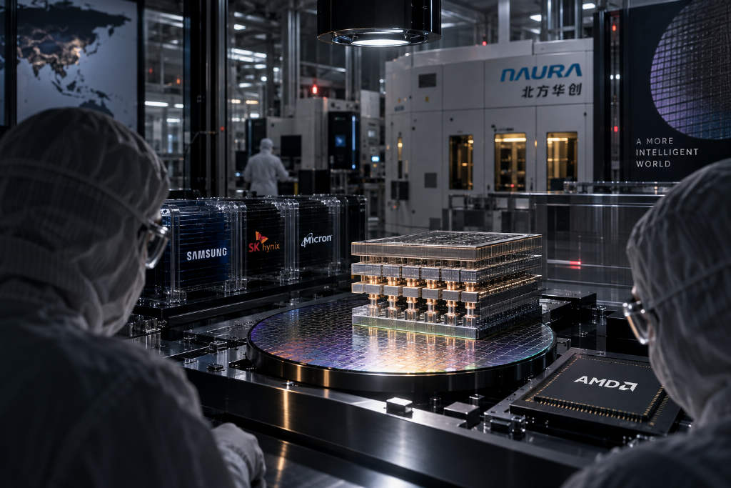
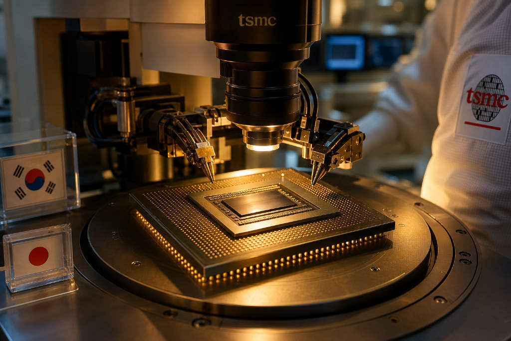
Competition in next-generation high-bandwidth memory, or HBM, is increasingly centered on advanced packaging rather than DRAM performance alone. A report cited by Damnang on Oct. 7, based on interviews with technical personnel, said SK hynix has run into difficulties developing hybrid bonding for future HBM, while Samsung Electronics has reportedly begun delivering samples using the technology to customers. The report did not identify the HBM generation, stack height, or customers involved, and it was not based on official statements from either company, leaving the actual development gap unclear.
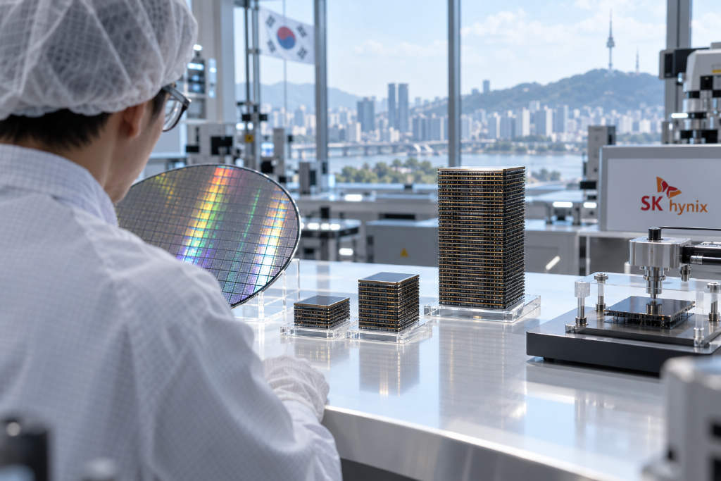
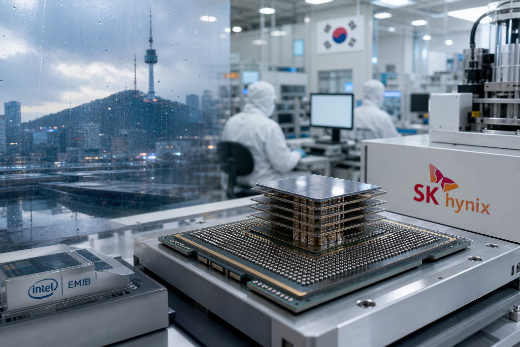
At the same time, SK hynix has continued to move forward with its existing packaging route. On June 18, the company said it had delivered 12-layer, 48GB HBM4E samples to major customers using its Advanced MR-MUF packaging technology, adding that thermal resistance improved by 17% versus HBM4. Samsung, for its part, introduced its hybrid copper bonding technology, HCB, on March 17 in materials tied to GTC-related events, saying the approach could cut thermal resistance by more than 20% compared with thermocompression bonding.
The central issue is no longer whether hybrid bonding works in a lab. The harder questions involve process stability, yield, cost, throughput, and customer qualification. Those factors, rather than sample delivery alone, will determine whether an early technical lead can become a durable commercial advantage.